William's Special Chip 1 (SC1, wiki page here). This is purportedly uses NMOS technology and is used in arcade blitting/DMA. To acquire these images Sean made a computer controlled microscope and was able to take a high resolution picture suitable for beginning to digitize the chip. (not all parts may be clear enough without delayering).
Here's a sample image from the chip:
This is upper left of the E3001 logo towards the center:
Tracing out polygons onto it:
With the following colors:
- Yellow: NMOS
- Blue: metal
- Red: polysilicon
- Green: buried contacts
- Black: contacts
Lets remove the image:
Looks cool but how to read it? I talked about PMOS a bit before with the Intel 4004, take a look here for some info on NMOS/PMOS.
Now with an idea on what things are, lets remove the irrelevant wires and add component labels:

Its fairly obvious looking at the layout what the two power rails are. Regardless if this was PMOS or NMOS VDD is the side with the resistors and VSS is the side that shorts out he pullups/pulldowns. Typically VSS is 0V and VDD is negative if PMOS or positive if NMOS. Since this is supposed to be an NMOS chip say VDD = V+.
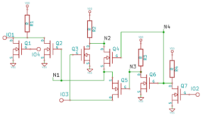
Converting to a schematic:
Rearranging:

Inverters are the easiest, lets start with those: R4 and Q7 form an inverter as when IO2 is not driving Q7 R4 pulls up N4 (0 in => 1 out). When IO2 asserts sufficient voltage on Q7 N4 is shorted to ground and the net goes low (1 in => 0 out). Similarly, R3/Q6 and R2/Q3 are inverters.
The area on the left is a little harder but not too bad. First, R1 is a pullup for IO1. If Q1 and Q2 never turned on the output would always be high.
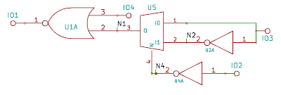
If either Q1 or Q2 turns on R1 is shorted to VSS. This means R1, Q1, and Q2 form a negative OR to yield:

Q4 and Q5 are still a little harder. At first it may not be clear if IO3 is an input or output. For example:
- Is the input on IO2/IO3 with the output ultimately on IO1?
- Is IO2 an input for a latch circuit feeding back into U2 that we can sense on IO3?
On the other hand, note that U3 inverts N4 to turn Q4/Q5 into complimentary transistors. That is, if one is on the other is off and vice versa. This means we are muxing the signals IO3 and N2 onto N1. This leads to:

This too bad as we are now completely into the digital domain. but we can simplify this further. First, U4 simply changes which of I0/I1 in mux U5 that we use. So if we switch I0/I1 U4 drops out. That leaves us with a function of IO2 that selects the inverse of IO3. That is if IO2 = 1 and IO3 = 1 then the mux selects the non-inverted I3 to give 1. If IO2 = 0 and IO3 = 0 then the inverted I3 is selected to give 1. In other cases we select the compliment of IO3 to yield 0. This gives us xnor:

Don't think this really simplifies much more so we are done!


No comments:
Post a Comment