I have a new microscope that yields way better images than anything I had before, but, unfortunately, I'm having some difficulty getting a camera hooked up to it nicely. In the meantime since I still have images from other sources I thought I'd take some time to go through some parts of the Intel 4004. Flylogic has a
similar write-up. This hopes to got a bit deeper especially showing how you can use tools to scale this up to analyze the/a full chip.
This article will use data from a variety of sources. The first is the
Intel 4004 35th anniversary page which I like since it explicitly lists material as
Creative Commons Attribution-Noncommercial-Share Alike 3.0 License. They also have a
composite image (this is the author of the 4004 website so I presume its under the CC license?), schematics, and other assorted information.
Datasheet and user manual can be found on Intel's website. I got the masks from
FPGA-netlist-tools and read them in CIF format, specifically
this file. if you don't want to load this up, you can find
the original here. Finally, I'm also going to use a few small excerpts from the
Flylogic top metal image and the
Flylogic delayered image which I think should be fine under fair use but will take down if they would rather not have them here. I thought Intel had some CC or related images (had maybe even contracted the Flylogic) job) but I can't find those now. If there are no freely available images, if someone wants to donate a 4004 I could release some under a free license of your choice (or three if you have a million: one top metal, one delayered, and one for my collection!).
According to Wikipedia, the 4004 is 10 um pMOS which I was also able to verify on
the datasheet ("4004 SINGLE CHIP 4-BIT P-CHANNEL MIROPROCESSOR"). This is similar to the NMOS logic I used in my JSSim inverter write-up except with the polarities reversed. Example PMOS inverter
here.
However, I started getting a little confused as I started to look through things.
Lajos describes pull-ups when I would expect PMOS to have pull-downs. Looking at various circuits, I also see what appears to be pull-ups. This confused me since I was thinking something along the lines of VDD = +5V, VSS = 0V with non-TTL compatible I/O (I didn't think through if the body connection is correct polarity, probably best to ignore it):

However, this doesn't really work since people would expect TTL compatible and this doesn't mask what I'm seeing in the mask as noted above. However, after looking at the user manual I found this:

Which shows that VDD = -10V and VSS = +5V which allows it to preserve TTL-compatible I/O. It was paired with this summary diagram:

The input stage shows why they want the +5V VSS: it provides the negative bias to trigger the PMOS input at 0 V while still allowing the pull-up to supply negative power for the input = 1 case. I was told that if you think of the circuit in terms of VDD, VSS, etc rather than actual voltages it should be more or less identical to NMOS logic. However, my understanding is that the depletion resistor is wired middle to bottom instead of middle to top so to speak as above. I don't have a good enough understanding of depletion modes to really know why this is the case.
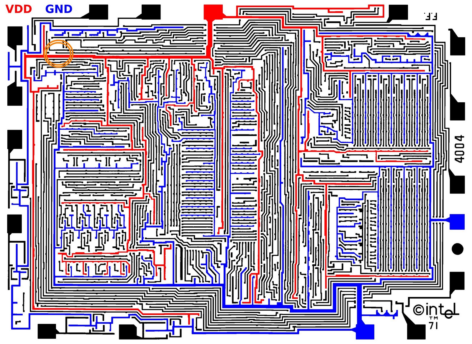
That cleared up, lets see an example. I decided to look at the upper left hand corner because it was convenient. Cross referencing with the schematic a particular signal such as TEST might have been more logical if I was following the schematic rather than focusing on the masks. Here's the
metal mask with VDD and VSS highlighted as well as an upper left hand corner area that I'll look at later in orange:

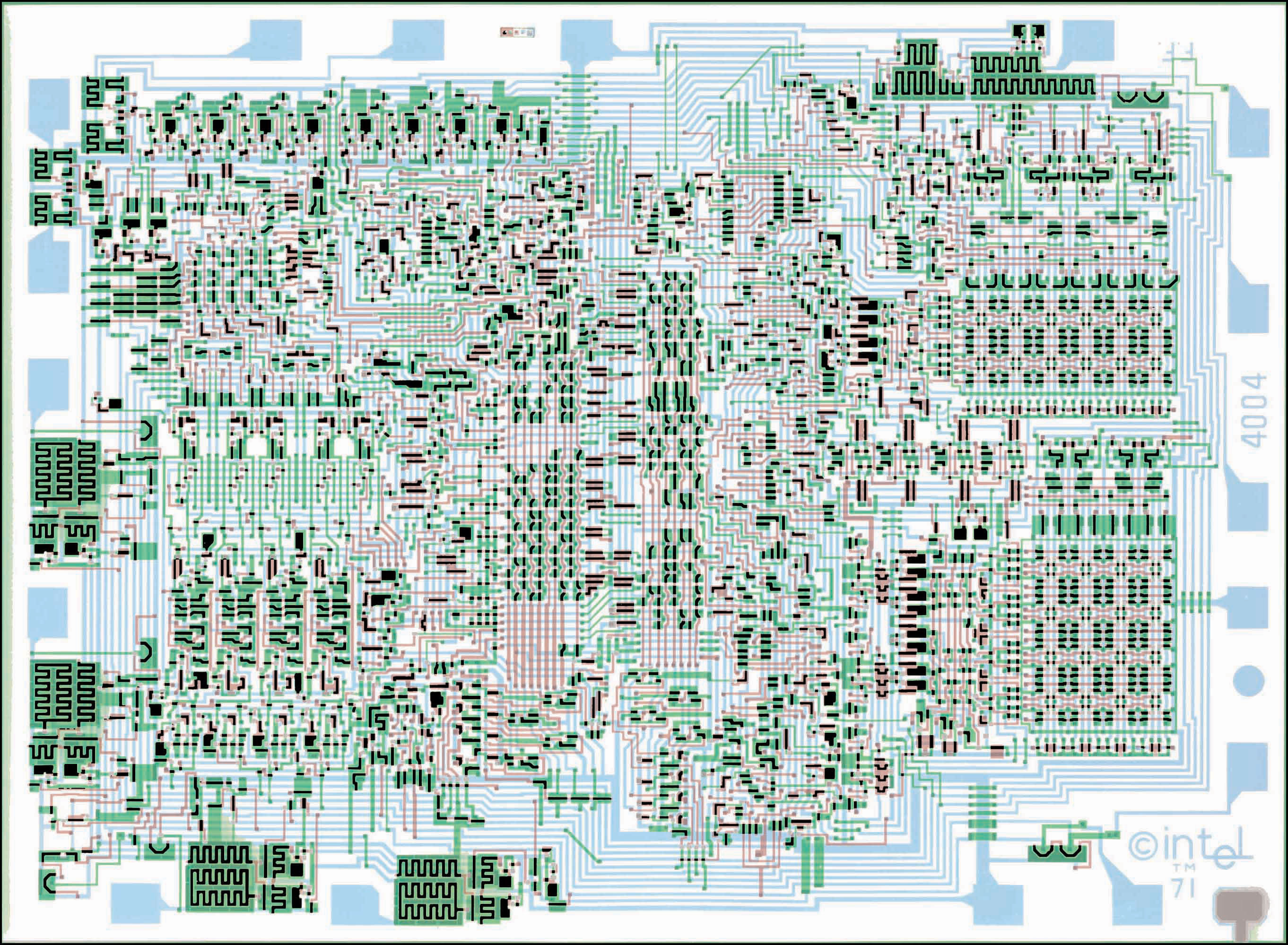
And a
complete version also marked, but without VSS/VDD highlight:

Lets start with a theoretical closeup. Here's a dump from my CIF rendering:
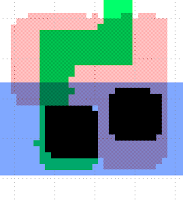
The red (okay so its pink, otherwise I had opacity related rendering issues) is poly, the green is diffusion, the blue is metal (VDD), and the black are contacts. So we have two contacts tied to VDD and one going elsewhere which forms our pull-up. Note that you might have a self aligned gate for an enhancement MOSFET, but for depletion the entire area is diffused for normally on behaviour. This is what it actually looks like (Flylogic) in metal:

If the poly had blocked the diffusion we would not have seen the diffusion squiggle inside of the poly area. If they poly and diffusion masks were reversed, we could still tell that they were layered vs blocked since we can see a change on the squiggle exit rather than a solid line. And after delayering:
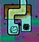
The poly and diffusion look almost identical. Fortunately, with whatever microscope technique they used (DIC maybe?) they get some good contrast between the traces and the background. I can't say for sure why it discolors where they meet, maybe just minor stress due to proximity.
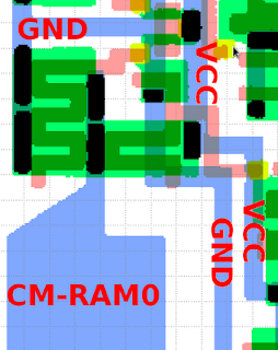
Okay, but one transistor is the middle of nowhere is kind of hard to follow, so lets take a look at some of the nearby pins and see how it fits in. The upper left hand corner ties in the CM RAM 0-3 pins increasing clockwise starting with CM RAM 0 and 1 on the left and 2 and 3 on top:

These pins essentially provide the chip (bank) selection outputs to the RAM chips (4002). Since you can operate the system with a single 4002 this is an optional pin. Nonetheless, its fine for demonstration purposes. Lets arbitrarily focus on CM-RAM 0. Detailed picture of its layout:
The first thing I did was label all of the transistors that looked like they were involved in this input stage:

There is an identical input stage above that shares a small bit of poly with Q4 (diffusion just visible), but this does not influence us so ignore it. I then created a schematic with transistors arranged like in the above:

This is fine for layout capture, but a little ugly to read. Lets rearrange it to something a little nicer:

And then simplify by converting transistors to resistors where appropriate:

Cross referencing against Lajo's schematic:
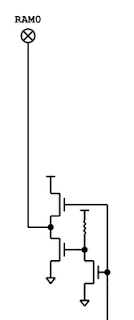
They are equivalent. I'm particularly happy with this because this would have taken me a long time before but I got this pretty quickly and without having to fudge anything.
Okay, but that's only part 1 where we've managed to reverse the mask into the schematic. For part 2 is we need to see if we could figure this out from just the optical image. Here's top metal:

And delayered:

Which I've just roughly cut by using a box select + copy/paste from the full size images. I could of course work with the full size images, but they are large enough that they take up a significant amount of memory.
Anyway, I then imported them into Gimp by creating a new, slightly oversized canvas (700 X 700), importing them as layers, and setting their opacity each to 50%:
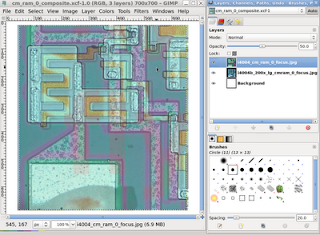
You'll notice the two images aren't quite aligned. This is why I wanted the oversize canvas as it allows me to move them around. Move them around until they line up. I should mention that I am by no means a Gimp expert, so don't take anything I do as to be the best was possible.
Next I created a layer for each mask. Since its difficult to tell buried contacts from contacts just by looking, I just created a single contacts layer (there there aren't any in our example). Since metal is very clear and un-ambiguous, I started with that by turning opacity back off and hiding the delayered image.
Press B to select the path tool. Click around a metal segment to form a polygon, remembering to click on the start portion to close it. You should now have a dashed line around your metal segment:
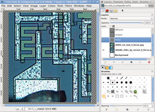
Then press shift-V to convert the path into a selection. Then press shift-B to select the fill tool and select a color (I used blue). Finally, fill the color in by clicking the mouse on the selection and then de-select your polygon by press ctrl-shift-A:

Make sure you put it on the metal layer by toggle show/hide for the metal layer. I believe this is the technique that was used to create the masks for the
visual-6800 (plus a tool that converted the masks to JSSim input). A few tips:
- You don't have to de-select the previous path. Just start working on the next one after fill and previous will automatically de-select when you convert it to a new path
- You don't need to close the polygon. Last and first points will be assumed to be connected
One metal is done contacts are good to do next. As we saw with the original pullup, diffusion and poly can be difficult to tell apart just by looking at them. However, we know that IC designers have specific goals, so we can use those to figure out which is which. That said, some ICs are obfuscated, but we'll ignore that for now. Poly will usually cross diffusion areas. In particular look for it jutting out to complete a diffusion cut-off. That said, in the Flylogic 4004 example poly tends to get a lot of brown discolouration while the diffusion does not.
My first cut looked like this:

A few issues:
- Need to figure out how to make level paths in Gimp so that it looks nicer. Right now it looks more like a kindergarten or abstract art drawing
- The bit of diffusion that forms the pullup is not connected. Cross referencing with the masks, it is suppose to jut out to the side to go to a buried contact / via stack. However in the image it looks pretty clearly to NOT do that to me as I clearly the the edge of the diffusion. Maybe I'll get some feedback to clear this up
- I also made an error with some poly to the right of this going to a buried contact, but this is visible in the images and a double check would have caught this. I also cared less since it wasn't part of the circuit I was analysing
- What is the stuff under the pad? Maybe diffusion, but its not in those masks. There is a matching passivation mask but that should be on top and this is on the lower layers
This is close enough to the original that I think I could have derived the same schematic although maybe with low confidence on the pullup part. The rest of the chip can be decoded be continuing this exercise.
Hopefully this served to augment the Flylogic article and not just repeat it. In any case it helped me to make sure I really understood it.


